Benvenuto alla Scenario.press - libera espressione
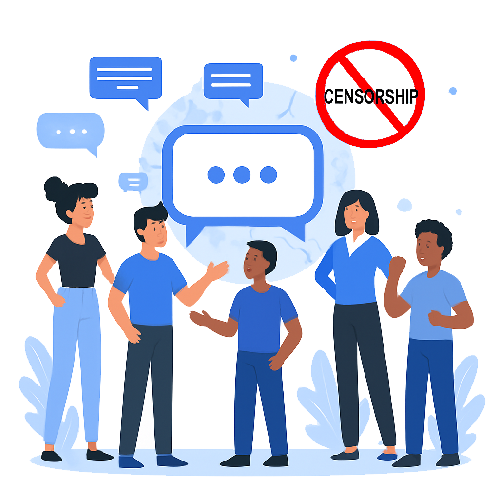
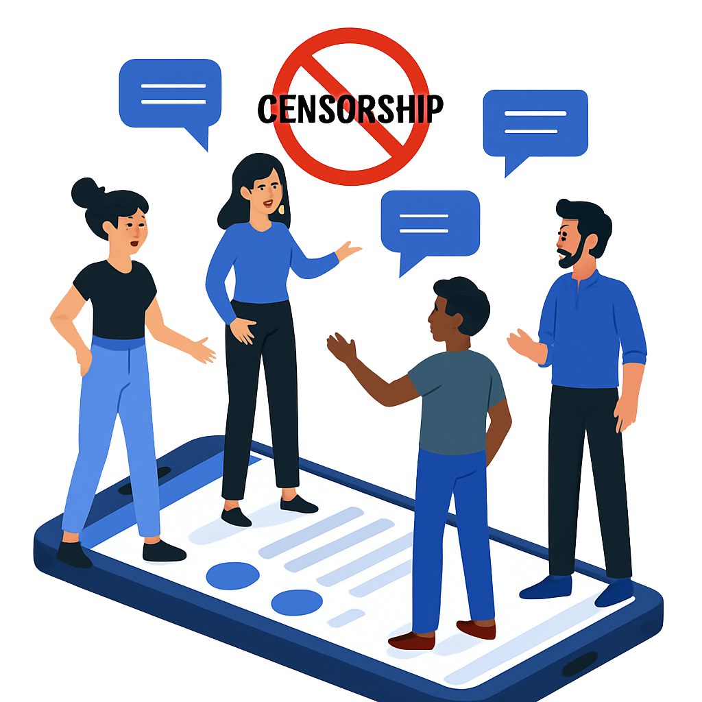
Benvenuto su Scenario.press - libera espressione - il primo Social Network Internazionale basato sulla fiducia delle persone. Vogliamo creare una rete di persone che possano conoscersi e interagire a livello personale. Siamo contro ogni forma di censura imposta dall'alto, siamo per la libertà di parola e di pensiero, siamo alla continua ricerca della verità! Welcome to Scenario.press - libera espressione - the first International Social Network based on people's trust. We want to create a network of people who can get to know each other and interact on a personal level. We are against any form of censorship imposed from above, we are for freedom of speech and thought, we are in constant search of the truth!

Accedi al tuo account
Bentornato! Inserisci i tuoi dati
o
Non hai ancora un account? Iscriviti
Puoi navigare liberamente in post, pagine, gruppi, eventi, utenti, ecc.

Sign Up for an Account
© 2026 Scenario.press - libera espressione
 Italiano